
Report an Error


NVIDIA RTX 6000 Ada Generation
- Graphics Processor
- AD102
- Cores
- 18176
- TMUs
- 568
- ROPs
- 192
- Memory Size
- 48 GB
- Memory Type
- GDDR6
- Bus Width
- 384 bit


GPU
I/O

Top
Recommended Gaming Resolutions:
- 1920x1080
- 2560x1440
- 3840x2160
The RTX 6000 Ada Generation is an enthusiast-class professional graphics card by NVIDIA, launched on December 3rd, 2022. Built on the 5 nm process, and based on the AD102 graphics processor, in its AD102 variant, the card supports DirectX 12 Ultimate. The AD102 graphics processor is a large chip with a die area of 609 mm² and 76,300 million transistors. Unlike the fully unlocked TITAN Ada, which uses the same GPU but has all 18432 shaders enabled, NVIDIA has disabled some shading units on the RTX 6000 Ada Generation to reach the product's target shader count. It features 18176 shading units, 568 texture mapping units, and 192 ROPs. Also included are 568 tensor cores which help improve the speed of machine learning applications. The card also has 142 raytracing acceleration cores. NVIDIA has paired 48 GB GDDR6 memory with the RTX 6000 Ada Generation, which are connected using a 384-bit memory interface. The GPU is operating at a frequency of 915 MHz, which can be boosted up to 2505 MHz, memory is running at 2500 MHz (20 Gbps effective).
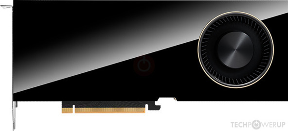
Being a dual-slot card, the NVIDIA RTX 6000 Ada Generation draws power from 1x 16-pin power connector, with power draw rated at 300 W maximum. Display outputs include: 4x DisplayPort 1.4a. RTX 6000 Ada Generation is connected to the rest of the system using a PCI-Express 4.0 x16 interface. The card measures 267 mm in length, 112 mm in width, and features a dual-slot cooling solution. Its price at launch was 6799 US Dollars.
Being a dual-slot card, the NVIDIA RTX 6000 Ada Generation draws power from 1x 16-pin power connector, with power draw rated at 300 W maximum. Display outputs include: 4x DisplayPort 1.4a. RTX 6000 Ada Generation is connected to the rest of the system using a PCI-Express 4.0 x16 interface. The card measures 267 mm in length, 112 mm in width, and features a dual-slot cooling solution. Its price at launch was 6799 US Dollars.
Graphics Processor
- GPU Name
- AD102
- GPU Variant
- AD102
- Architecture
- Ada Lovelace
- Foundry
- TSMC
- Process Size
- 5 nm
- Transistors
- 76,300 million
- Density
- 125.3M / mm²
- Die Size
- 609 mm²
Graphics Card
- Release Date
- Dec 3rd, 2022
- Availability
- Jan 20th, 2023
- Generation
-
Workstation Ada
(x000A)
- Predecessor
- Workstation Ampere
- Successor
- Blackwell PRO W
- Production
- Active
- Launch Price
- 6,799 USD
- Bus Interface
- PCIe 4.0 x16
Relative Performance
Based on TPU review data: "Performance Summary" at 1920x1080, 4K for RTX 3080 and faster.
Performance estimated based on architecture, shader count and clocks.
Clock Speeds
- Base Clock
- 915 MHz
- Boost Clock
- 2505 MHz
- Memory Clock
-
2500 MHz
20 Gbps effective
Memory
- Memory Size
- 48 GB
- Memory Type
- GDDR6
- Memory Bus
- 384 bit
- Bandwidth
- 960.0 GB/s
Render Config
- Shading Units
- 18176
- TMUs
- 568
- ROPs
- 192
- SM Count
- 142
- Tensor Cores
- 568
- RT Cores
- 142
- L1 Cache
- 128 KB (per SM)
- L2 Cache
- 96 MB
Theoretical Performance
- Pixel Rate
- 481.0 GPixel/s
- Texture Rate
- 1,422.8 GTexel/s
- FP16 (half)
- 91.06 TFLOPS (1:1)
- FP32 (float)
- 91.06 TFLOPS
- FP64 (double)
- 1,422.8 GFLOPS (1:64)
Board Design
- Slot Width
- Dual-slot
- Length
- 267 mm
10.5 inches
- Width
- 112 mm
4.4 inches
- TDP
- 300 W
- Suggested PSU
- 700 W
- Outputs
- 4x DisplayPort 1.4a
- Power Connectors
- 1x 16-pin
Graphics Features
- DirectX
- 12 Ultimate (12_2)
- OpenGL
- 4.6
- OpenCL
- 3.0
- Vulkan
- 1.3
- CUDA
- 8.9
- Shader Model
- 6.8
Card Notes
| 3 NVENC Engines 3 NVDEC Engines |
AD102 GPU Notes
| Ray Tracing Cores: 3rd Gen Tensor Cores: 4th Gen NVENC: 8th Gen NVDEC: 5th Gen PureVideo HD: VP11 VDPAU: Feature Set K Latest Drivers: Windows 10 / 11: GeForce Release: Latest Quadro Release: Latest Data Center Release: Latest |
Retail boards based on this design (1)
| Name | GPU Clock | Boost Clock | Memory Clock | Other Changes |
|---|---|---|---|---|
| 915 MHz | 2505 MHz | 2500 MHz |

Jul 17th, 2025 21:42 +08
change timezone
Latest GPU Drivers

New Forum Posts
- computer unstable after case swap (13)
- Can this Z690 mobo be saved with three broken pins? (2)
- AI Job Losses: let's count the losses up, total losses to AI so far 94,000 and counting (23)
- Microcenter GPU Stock status (170)
- Why Aren't USB C Video Cables More Common (2)
- VR Health and Exercise Apps (15)
- A beeping sound is heard when gaming on a 9070 XT, need a fix (not a coil whine) (6)
- PLS the right Bios.... (5)
- R-T-B's house of Hisense Firmware (0)
- Adding distilled water to ups batteries really work ? (36)

Popular Reviews
- MSI GeForce RTX 5060 Gaming OC Review
- SilverStone SETA H2 Review
- Pulsar X2 Crazylight Review
- Our Visit to the Hunter Super Computer
- NVIDIA GeForce RTX 5050 8 GB Review
- Lexar NM1090 Pro 4 TB Review
- Sapphire Radeon RX 9060 XT Pulse OC 16 GB Review - An Excellent Choice
- Upcoming Hardware Launches 2025 (Updated May 2025)
- AMD Ryzen 7 9800X3D Review - The Best Gaming Processor
- Fractal Design Epoch RGB TG Review
TPU on YouTube
Controversial News Posts
- Intel's Core Ultra 7 265K and 265KF CPUs Dip Below $250 (288)
- Some Intel Nova Lake CPUs Rumored to Challenge AMD's 3D V-Cache in Desktop Gaming (140)
- AMD Radeon RX 9070 XT Gains 9% Performance at 1440p with Latest Driver, Beats RTX 5070 Ti (131)
- NVIDIA Launches GeForce RTX 5050 for Desktops and Laptops, Starts at $249 (122)
- NVIDIA GeForce RTX 5080 SUPER Could Feature 24 GB Memory, Increased Power Limits (115)
- Microsoft Partners with AMD for Next-gen Xbox Hardware (105)
- NVIDIA DLSS Transformer Cuts VRAM Usage by 20% (99)
- AMD Sampling Next-Gen Ryzen Desktop "Medusa Ridge," Sees Incremental IPC Upgrade, New cIOD (97)